
| Name: | HDI PCB |
|---|---|
| Surface finish: | Immersion Gold(ENIG) |
| Finished copper thickness: | 1OZ |
| Material: | FR4(Tg170℃) |
| Layer: | 6 |
| Finished board thickness: | 1.2mm |
| Min hole size: | 0.2mm |
| Solder mask color: | Blue |
| Silkscreen color: | white |
Product Description
HDI (High Density Interconnector) PCB
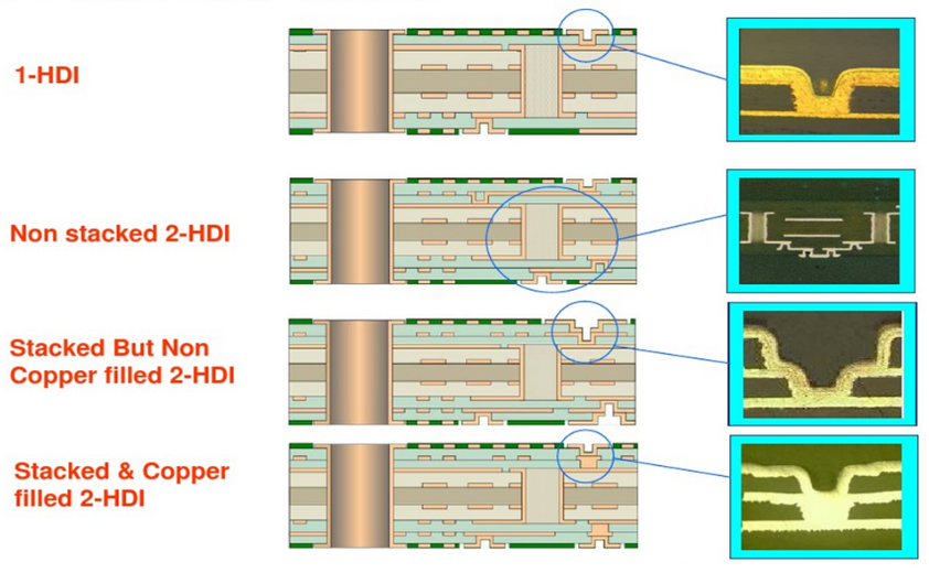
Laser via and Blind via design,reduce PCB cost,increase conductor density, better electrical performance and signal correctness,reduce RF interference
Applications include mobile phone,digital camera,MP3,MP4,notebook computer and automotive.
In Vip Circuit, with advanced production equipment, excellent PCB solutions and complete testing methods, we have specialists working on their particular fields with the thorough mastery of their particular discipline in each of the production facilities. Training, as well as technical exchanges, are held frequently, tackling problems in key technologies and configuring scheme of equipment and allowing professionals to get up to speed on the essential tools that many organizations value today in the manufacturing industry. Thanks to those above, we have greatly improved the strength and won international reputation.
Technology Summary
| PCB Features | Ø PCB with up to 30 layers | Ø Impedance control |
| Ø Flex PCB up to 6 layers | Ø Via plugging/Laser hole stacking | |
| Ø Aluminum core | Ø Special material | |
| Ø Heavy copper(power boards) | Ø Hybrid (RO4350+FR4) | |
| Ø Blind and buried Vias | Ø Gold plated | |
| Ø HDI | Ø Min hole 0.2mm | |
| Ø RF(High frequency) | Ø Max copper thickness 6oz | |
| Surface Treatment | HASL/LF HASL | |
| ENIG/ENEPIG | ||
| Immersion Tin | ||
| Immersion Silver | ||
| OSP | ||
| Gold Finger/Gold plated | ||
| Selective Chem Au | ||
| Material | FR-4 |
CEM-1 |
| Halogen-free | PTFE | |
| Rogers | Polyimide | |
| Arlon | Hybrid | |
| Isola | BT | |
| High TG | Ceramic filled | |

Related Products

10-layer interconnected H...

10-layer PCB 2+N+2 HDI-...

HDI PCB
 Send Email
 Jeff
JeffLiveChatclose