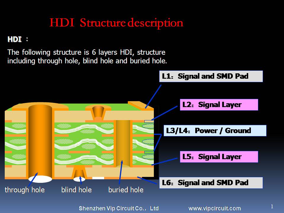
HDI PCB application and processing flow

HDI PCB full name is High Density Interconnection Print Circuit Board,a kind of print circuit board with high density of distribution lines using micro blind buried hole technology.HDI PCB is characterized by small and  thin, so it is widely application on cellphone,Tablet PC,Wrist Watch,Digital camera,Notebook computer and so on.
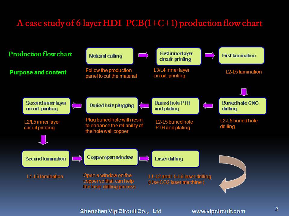
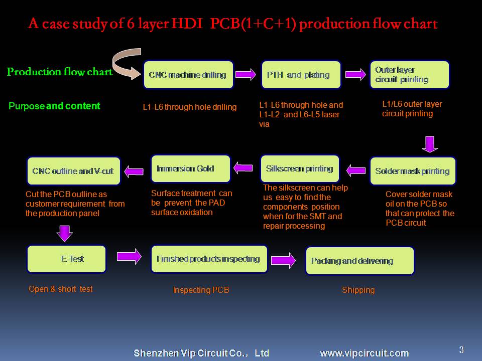
Here I will use an example to illustrate HDI PCB's processing flow,a case study of 6 layer HDI  PCB(1+C+1) production flow chart,please see the following picture for detail:


Print
Categories