Ten quality problems and solutions for PCB manufacturing
In the entire PCB manufacturing process, there are a lot of control points, there is a little bit of careless, the board will be broken, PCB quality problems are varied, due to the long production process, this is a headache, only one piece has a problem, then most of the components will also cannot use.I have compiled a total of ten issues, listed here and attached some experience to deal with. Share with you.
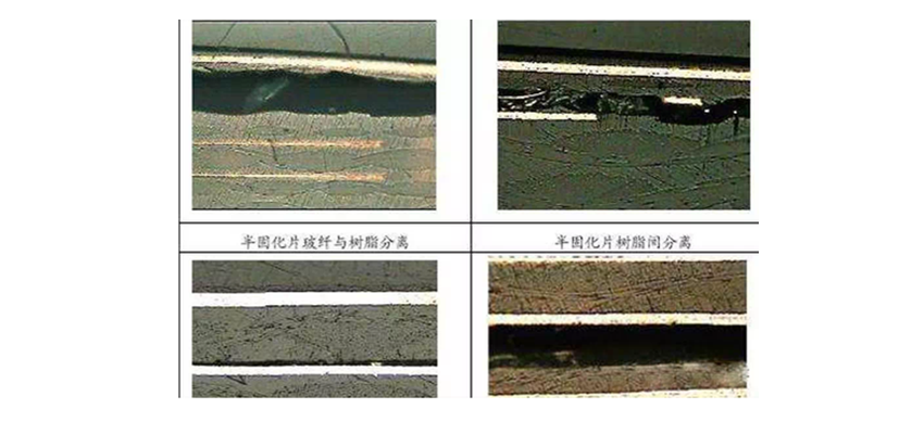
1. Delamination (Layer separated)
(1) Improper packaging or preservation, affected with damp
(2) Long time to save, more than the shelf life, PCB board is damp
(3) Supplier material or process problems
(4) Design materials problems or copper surface distribution is poor
Vacuum conductive bags or aluminum foil bags can be a good protection of water vapor intrusion. If there is a problem with the raw material or process of the product, the probability of being scrapped is quite large. Common possible causes include, black-oxide is bad, pp or inner layer is damp, pp gum volume is not enough, abnormal pressure etc.
In order to reduce this situation, special attention should be paid to the PCB supplier management of the corresponding process and the layered reliability test. For example the thermal stress testing, a good factory standard requires more than 5 times not to be layered, in the sample stage and the production of each cycle will be confirmed, and ordinary factory standards may be only 2 times, a few months to confirm once. The IR test can also be more to prevent the outflow of non-performing products, is an excellent PCB manufacturing factory must be.
Certainly, the design company's own PCB design will also bring hidden dangers of layering. For example, the choice of TG, for ordinary TG materials, temperature resistance will be relatively poor. In addition, the open large copper surface and too dense buried hole area is the hidden danger of PCB layering, need to avoid in the design.
2. Poor Solderability
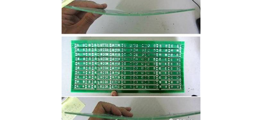
3. Board Warping
4. Scratch& Copper exposed

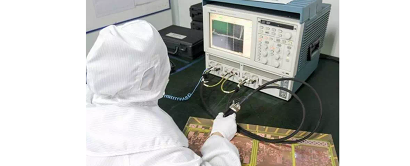
5. Bad Impedance
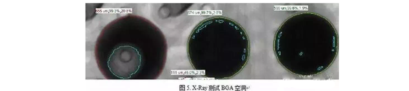
6. BGA Solder Hollow
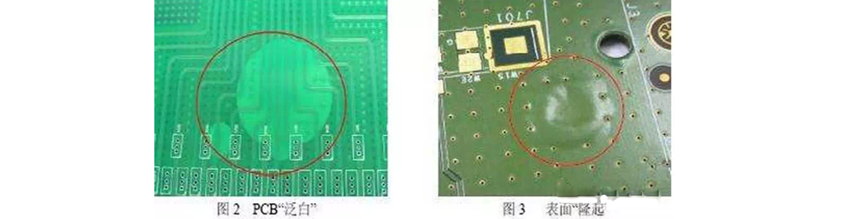
7. Soldermask foaming/shedding
8. Poor hole plugging
9.Bad size
There are many possible reasons for the poor size, PCB manufacturing process is prone to shrinkage, the supplier adjusted drilling procedures/graphics ratio/forming CNC program, may cause the mount prone to bias, structural parts with poor assembly. This type of problem can only be controlled by the supplier's good process, so you need to pay special attention to select PCB supplier.
10. Galvanic Corrosion
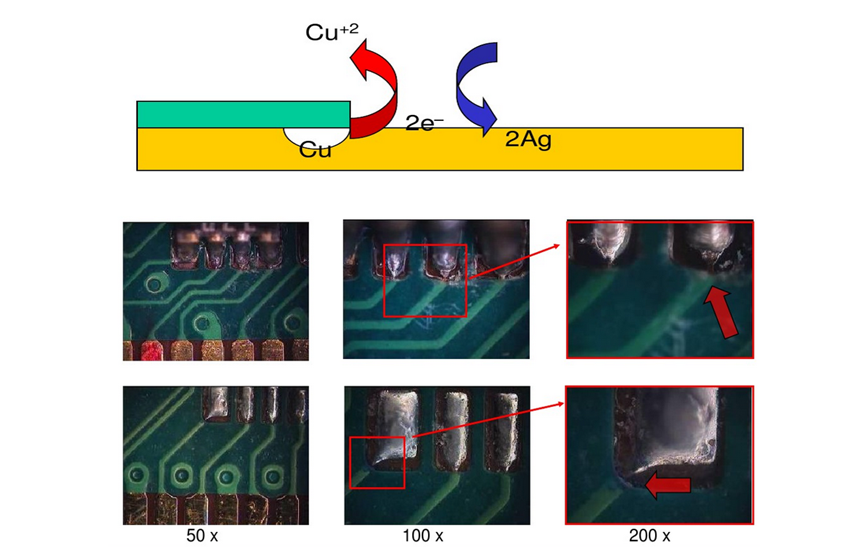
Experienced PCB factory will be through computer software screening this part of the pad, Pre-compensation at design time, and setting conditions in the process to avoid problems occur. So this issue needs to be checked out a good PCB manufacturer.
Find a reliable and experienced PCB supplier can meet your any custom PCB requirements, high reliable quality assurance! Welcome visit VIP CIRCUIT.
【Print】
 Send Email
 Jeff
Jeff